DFI is a company that needs no introduction, especially with the PC enthusiast community. Just about any overclocker can remember getting excited about the very popular nForce 2 based ‘Ultra B’ several years ago and the more recent award winning LanParty NF4 based boards. Although the LanParty series of boards are DFI’s flagship, today we’ll be looking at the more budget minded Infinity NF570 M2/G.
DFI’s Infinity series of boards are often less elaborately ‘dressed’ than their LanParty counterparts but enthusiasts have noticed time and time again that the boards “have it where it count”. Features like UV-reactive plastic components, rounded IDE cables, multiple SATA controllers, dual NICs and Karajan based audio modules are just some of the features that will not be found with the Infinity series of boards. What you can expect to find, however, is just about everything else that lies beneath those ‘nifty’ extras—a quality board designed by a company with a rich overclocking heritage.
|
|
Designed around the nForce 570 MCP for the AMD AM2 platform, the Infinity M2/G promises to deliver a healthy array of ‘useful’ features for a reasonable price—and of course, the tweakability you’ve come to expect from DFI. There are actually two Infinity NF570 M2/G models in DFI’s lineup. The one we will be looking at today is the one based on the nForce 570 Ultra MCP. The other slightly more expensive model is the nForce 570 SLI based M2/G—which is nearly identical.
Mainboard Specifications
Taken from the DFI site
- CPU
- AMD Athlon 64 FX / Athlon 64 X2 / Athlon 64 / Sempron
- Socket AM2
- HyperTransport
- 2000MT/s HyperTransport interface
- Chipset
- NVIDIA nForce 570
- System Memory
- Four 240-pin DDR2 DIMM sockets
- Supports DDR2 533, DDR2 667 and DDR2 800 DIMMs
- Supports dual channel (128-bit wide) memory interface
- Supports up to 8GB system memory
- Expansion Slots
- 2 PCI Express x16 slots (PCIE 1 slot operates at x16 bandwidth, PCIE 3 slot operates at x1 bandwidth)
- 1 PCI Express x1 slot
- 3 PCI slots
- BIOS
- Award BIOS
- 4Mbit flash memory
- Power Management
- ACPI and OS Directed Power Management
- ACPI STR (Suspend to RAM) function
- Wake-On-PS/2 Keyboard/Mouse
- Wake-On-LAN
- RTC timer to power-on the system
- Hardware Monitor
- Monitors CPU/system/chipset temperature
- Monitors 5V/12V/Vcore/Vbat Dual voltages
- Monitors the speed of the cooling fans
- CPU Overheat Protection function monitors CPU temperature during system boot-up
- Audio
- Realtek ALC882 High Definition audio CODEC
- 8-channel audio output
- S/PDIF interface
- LAN
- NVIDIA® chip integrated with Gigabit MAC (Media Access Control) technology
- Marvell 88E1115 Gigabit Phy
- Fully compliant to IEEE 802.3 (10BASE-T), 802.3u (100BASE-TX) and 802.3ab (1000BASE-T) standards
- IDE
- One IDE connector allows connecting up to two UltraDMA 133Mbps hard drives
- Serial ATA with RAID
- Six Serial ATA ports
- SATA speed up to 3Gb/s
- RAID 0, RAID 1, RAID 0+1 and RAID 5
- IEEE 1394
- VIA VT6307
- Supports two 100/200/400 Mb/sec ports
- Rear Panel I/O
- 1 mini-DIN-6 PS/2 mouse port
- 1 mini-DIN-6 PS/2 keyboard port
- 1 optical S/PDIF-out
- 1 RCA S/PDIF-out
- 1 parallel port
- 1 COM port
- 1 IEEE 1394 port
- 1 RJ45 LAN port
- 4 USB 2.0/1.1 ports
- Line-in, line-out (front R/L) and mic-in jacks
- Center/subwoofer, rear R/L and side R/L jacks
- Internal I/O
- 3 connectors for 6 additional external USB 2.0/1.1 ports
- 1 connector for 1 external IEEE 1394 port
- 1 front audio connector for external line-out and mic-in jacks
- 1 CD-in internal audio connector
- 1 S/PDIF connector for optical cable connection
- 1 IrDA connector
- 6 Serial ATA connectors
- 1 IDE connector
- 1 floppy connector
- 1 24-pin ATX power connector
- 1 8-pin ATX 12V power connector
- 1 4-pin 5V/12V power connector (FDD type)
- 1 front panel connector
- 5 fan connectors
- EZ touch switches (power switch and reset switch)
- PCB
- ATX form factor
- 22cm (8.66″) x 30.5cm (12″)
Packaging and Accessories

The accessory bundle included with the NF570 M2/G is a bit weak, but not outside what I’d expect at this price point. For included ‘frill’, you’ll have to look to the Lanparty series of boards. Simple and functional is what you’ll get with an ‘Infinity’ series board.

The included DFI disc comes with drivers for audio, SATA RAID, AMD Cool n’ Quiet and the ForceWare drivers. These will do in a pinch, however, I’d definitely recommend getting the latest drivers from the respective manufacturer sites. Also included is the ‘ITE Smart Guardian’ monitoring application and a PDF copy of the owner’s manual. A special note must be made about the DFI owner’s manual—It is very thorough and well written. Any questions you may have surrounding installation will likely be answered in the manual.
nForce 570 Revisited
Although the nForce 500 series is not new, released back in May of 2006 along side the AM2 platform, it is still the most popular chipset series for the AM2 platform. Nvidia packed a lot of functionality into the NF500 MCPs. I won’t bore you with a lengthy technical overview of the NF500 features but I think it is important to mention some of the features that ‘come standard’, so to speak.

Unlike the nForce 590 flagship, the nForce 570 is a single chip solution that provides an interface for PCI/PCI-E, USB, Audio, SATA, IDE and more. The NF570 is a popular choice due to it retaining many of the great features found in the NF590 like rich networking and storage features.
The NF570 network controller supports nVidia’s implementation of QoS called ‘FirstPacket’ technology. The nVidia driver allows the prioritization of traffic based on application types. An online game should theoretically get higher network priority than an FTP client for example—a useful feature if you are a heavy multitasker. Another useful feature that the NF570 provides is ‘TCP/IP Acceleration’, which simply offloads some of the work that the CPU needs to do to the MCP. Although the NF570 does support dual NICs and ‘Teaming’ (the logical joining of two NICs into a single virtual NIC for greater bandwidth and redundancy), the DFI NF570-M2/G only has a single physical NIC so this feature will not be available.
The NF570 also has the same full-featured storage controller that the NF590 benefits from. It natively supports six SATA2 drives in a variety of RAID configurations, including RAID-5 and RAID-0+1. It also allows you to have a combination of RAID levels, like two separate volumes with three drives in RAID-0 and three drives in RAID-5 for example. The IDE channel can also be used in a RAID configuration for very flexible RAID options. As an added benefit, this chipset based RAID controller enjoys performance beyond what is possible with PCI or 1x PCI-E based controllers found on lower-end boards. High STR (sustained transfer rates) should be possible from striped volumes spanning multiple disks on chipset based RAID controllers.
Aside from SLI support, the NF570 has fewer PCI-E lanes (20 down from 46) compared to the NF590 as well as the lack of features like ‘Link Boost’, which only minutely benefits SLI configurations. So, if you only plan to use a single graphics card, the NF570 is an excellent, full-featured choice.
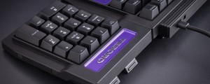
Board Layout


Board diagram taken from the DFI Infinity NF570-M2/G Owner’s Manual
The overall layout of the NF570-M2/G is good. The ATX 24-pin connector and the 8-pin +12V connector are both located at the top right corner of the board, which is my preference. The IDE connector is also in a good location at the upper half and right side of the board. The floppy connector is not in an ideal location at the bottom of the board but considering how few people use floppies these days, I’d be thankful there is one included at all. At first glance, something looked very familiar about the overall layout of the NF570 M2/G—I was not imagining it.

Above is a shot of my DFI NF4 Expert—a board that implemented some key layout improvements over the popular SLI-DR and Ultra-D boards of the same era. Obviously, it is not identical, but the same overall scheme was clearly inspired by this board. Dual slot spacing between the PCIE-16x slots and better placement of the chipset and fan were important improvements. This design, unfortunately, does have some disadvantages as well. The spacing between the CPU socket and memory is too narrow—this poses a problem with some large coolers. The problem is worse with the NF570-M2/G as there is actually even less space than the NF4 expert in this area. The second problem is the close proximity of the first PCIE-16x slot to the memory slots and to the CPU socket—again, a potential problem for very large coolers. It would have been nice to see alternating DIMM channels and spacing between the pairs as was done in the NF4 expert. Overall, these are pretty minor gripes and will not be a problem for most users. Overall, the layout is good.
The M2/G employs the 4-pin floppy style power connector above the first PCI-E slot just like the NF4 expert as well. The DFI manual indicates that this is only necessary when running dual graphics cards in an SLI configuration, but will “improve overall system stability” so it is definitely in your best interest to use it. The 8-pin +12V connector will accept a 4-pin input without issue, although the retaining clip does not work so you’ll have to ensure your 4-pin connector is fit snugly into the connector. I’m still using my good old PC Power and Cooling 510 express with a 4-pin +12V connector.

The SATA connectors are located at the very edge of the board and are plugged in horizontally, not vertically like most boards. The floppy connector is also oriented in this way. This allows for cleaner installation but also poses some problems in certain cases like my Lian-li PC-65 where the hard drive cage interfered with protruding SATA cables. If this is a problem, right-angled SATA cables can be purchased from your favourite online retailer and should solve the problem. This should not be a problem with most mid-tower ATX cases. The NF5 series of boards has reduced the number of IDE channels to only one but has included six SATA2 ports standard. As can be seen here, there are also three internal USB headers rather than two with the older NF4 boards.

It was nice to see some unexpected extras on the NF570 M2/G including IEEE 1394 support and both optical and coaxial S/PDIF. There is a fair bit of legacy retained on the board as well with PS2 mouse/keyboard and parallel/serial ports included. These ports are becoming exceedingly rare these days.

As mentioned previously, the two-slot spacing between the PCIE-16x slots is a positive feature. The chipset cooler does not interfere with longer cards like the 8800GTS. Although this board does not support SLI, the layout is the same as the SLI version of this board. The blue PCIE slot is functional in the vanilla M2/G, but limited to only 1x operation—not suitable for a modern graphics card. The SLI version of the M2/G has greater bandwidth available to the second PCIE slot (8x) and an included SLI bridge. Aside from that, they are pretty much identical.

A popular feature from the Lanparty series of boards was maintained—the onboard power/reset switches. These are very handy if you are doing some testing outside of a case. There is also an onboard PC-Speaker and colour coded LED/switch headers. Three internal USB headers is also a nice plus. The clear CMOS jumper is JP4 located just to the right of the first USB header (always important to get acquainted with this one).

The DFI ‘Magnetic Levitation’ fan has become a familiar sight across many of their boards. Although it can spin upwards of 7000RPM, it is relatively quiet at about 50% operation and sports a very high MTBF (mean time before failure). It does a decent enough job keeping the NF570 MCP cool.

Power regulation is provided by a 3-phase PWM design similar to what we have seen on the NF4 based DFI boards. Although it may not sound as impressive as some of the new 8-phase designs by ASUS or DFI’s own digital PWM solutions, it is a tried and tested design. The NF570 M2/G does not employ solid-state capacitors like some of the Lanparty boards, but the capacitors appear to be of a higher quality variety. There are no passive coolers on the mosfets, unfortunately. This might be something a DIY’er may wish to add on at a later date. This area of the board does get pretty hot when testing hardware limits so it would be wise to find a way to get some airflow in this area if you are seriously pushing your gear. Downdraft CPU coolers do help to keep this area cool, but the tower varieties do not.

The NF570 M2/G supports the newer 4-pin CPU fans and is backwards compatible with the more common 3-pin varieties.

The onboard gigabit Ethernet port is made possible by a Marvel 88E1115 PHY as seen here. The 4-pin floppy power connector is also visible to the right of the image above. IEEE 1394 support is also included courtesy of a VIA VT6307 chip.

Onboard audio utilizes the Realtek ALC882 high definition CODEC. Although it is certainly not the best on the market today, it is actually a very decent codec to find on a value priced board. It is noticeably better than the ALC850 found on the NF4 series Lanparty boards.
Test Configuration
The system used for testing consists of the following:
- AMD Athlon 64 X2 6000+
- Thermalright SI-128 SE heatsink (Panaflow ‘High’ 120mm fan)
- 2x1GB Buffalo Firestix PC2-6400 DDR2 (Micron D9GMH)
- DFI Infinity NF570-M2/G Mainboard
- BFG nVidia 8800GTS 640MB OC
- Western Digital Caviar WD3200AAKS SATA2 Hard Drive (Operating System)
- Seagate 7200.7 160GB SATA (Storage)
- Pioneer DVR-108 IDE DVD Drive
- PC Power and Cooling 510 Express PSU
- Lian-Li PC-65B
- Windows XP Professional (32 bit) SP2 with all hotfixes installed as of 9/10/07

As can be seen here, the area around the socket is tight with large 120mm coolers like the SI-128 SE, but still manageable. The NF570’s first RAM slot was obstructed a millimetre or two using the SI-128 SE, so I had to use the slots furthest from the CPU socket. Again, this will not be a problem for most people as this is a very large heatsink.

I should also mention that the NF570-M2/G does not have an OEM backplate included. It uses pressure clips as can be seen here. These clips do secure well but it would have been preferable to have a backplate included. The area behind the socket is pretty clear and should not interfere with 3rd party backplates. I had no issues using the Thermalright SI-128SE’s backplate with the NF570-M2/G. The only potential problem this could cause is with heatsink manufacturers that provide mounting hardware that assumes an OEM backplate can be reused. Thankfully, this is not usually an issue.
It is also important to note that the NF570-M2/G started up right away without issue. It posted normally at the first try with the above mentioned hardware configuration.
The BIOS
The NF570-M2/G did not recognize my ‘Windsor’ based 6000+ processor with the shipping BIOS revision. It was listed as ‘unknown model’ at each boot, however it worked just fine. A quick flash to the latest BIOS corrected this.

The NF570 M2/G uses the very familiar ‘Award’ BIOS, similar to what is found on just about all DFI boards. One feature that I absolutely loved on the NF4 series of boards was missing, however, CMOS Reloaded! Even though this is not a Lanparty series board, it would have been nice to see that feature passed down.

All of the legacy configuration can be found in the ‘SuperIO Device’ menu. Call me a minimalist but if I’m not using it, I’m disabling it!

Plenty of PM parameters can be set, as we would expect from any brand name board.

System monitoring can be done from the ‘PC Health Status’ menu. Fan speed can be set here as well as safety shutdown temperatures. Interestingly the fan labelled ‘System Fan’ is not the header closest to the top of the board like with most of DFI’s offerings. It is the header found at the bottom most part of the board.


The ‘Genie BIOS’ menu is where all of the magic happens. Parameters relevant to overclocking reside here: voltage options, DRAM configuration and clock frequencies. One very nice feature is the automatic display of CPU and memory clock speed before having to save and quit. You won’t need a calculator to find your memory clock speed when using dividers. DFI did not provide this for the HTT frequency but as you’ll see later, HTT stability is not an issue with this board. You can also view the CPU, DRAM, Chipset and HT voltage readings from this menu.


True to what we expect from DFI, a whole slew of memory timings are available for tweaking. Everything from CAS latency to drive strength to ‘CS/ODT Fine Delay’ is available—don’t ask me what that last one does.


As can be seen here, the full range of multipliers is available for HTT and CPU.

I love the ‘type-in’ reference clock selection. Just type in the number and away you go. I don’t know why more board manufacturers don’t include this.

The PCI-E frequency clock is adjustable from 100MHz to 145MHz, although this is not something most users will want to increase.

CPU voltage is adjustable from 0.8V all the way to 1.85V—plenty for even the most extreme overclocks. Most individuals will not push CPU voltage beyond 1.6V. Even with my Vapochill LS, I have never needed to exceed 1.65V on a 90nm AMD processor. Nice to know its there, none the less.

DRAM voltage or vDIMM can be set as high as 2.5V. Although this is not as extreme as the 3+ volts available on the Lanparty NF590 based board, it is plenty to get your Micron D9 based modules cooking and more than enough to damage your memory if you are not careful. This is about what I would expect to find on flagship boards from other manufacturers and beyond what is expected from a value priced offering.

The NF570 MCP can be overvolted by 0.3V. In my testing, 1.5V was plenty for very high reference and HTT clocks.

Some PCI-E lane configuration can be done as can be seen here. I didn’t get a chance to try these options but I can confirm that the second PCI-E graphics slot is severely bandwidth limited. According to DFI, it is limited to 1x operation on the non-SLI version of this board. The first full size PCI-E slot operates at 16x.
Performance
Since this is the first AM2 based board Icrontic has reviewed, we do not have other boards available for comparative analysis yet. This section will be updated in the future once we have a testing methodology and other boards.
Overclocking
True to the reputation DFI has built, the NF570 M2/G is capable of some very impressive numbers. I was able to achieve an incredible 418MHz reference clock speed—a 109% overclock from the 200MHz default. As you can see in the below screenshot, this 6000+ CPU was overclocked to 3.35GHz with an 8x multiplier. The board would not post with a 1MHz increase beyond 418MHz. I was very sceptical about the overall system stability at these very high reference clock speeds so I did what any overclocker would do—I played Quake 3. Since this 6000+ is not totally stable at 3.35GHz, I decreased the reference clock to 400MHz (still a 100% increase over default) which yields a stable 3.2GHz. I launched Quake 3 in a window and played while an instance of SuperPI 1.5 (32M) ran along side it. The system was rock-solid at 8×400—just amazing. Multipliers below 8x did not yield the same results, but could still be pushed very close to the 400MHz line. It is safe to say that the NF570 M2/G will not be the bottleneck when you try to push your AM2 processor to the limits. To put this number into perspective, a board capable of a 300MHz reference clock is usually considered to be an ‘overclocker friendly’ board–418MHz is just incredible. Even with the lowest end AM2 processors available today, you’d still be working with at least a 9x multiplier. A 3.6+GHz overclock would theoretically be possible with this board and a CPU with a 9x multiplier. Bravo, DFI!

|

Another interesting observation I made was the behaviour of the ‘HTT multiplier’ on the NF570 platform. With the older NF4 based boards the HTT bus had to be kept as close as possible to the 1000MHz default frequency to maintain stability—this is not the case with the NF570. I was able to push the HTT bus very high at the 4x and 5x HTT multipliers. The board was completely stable with HTT bus speeds in excess of 1600MHz. Interestingly; stability actually improved at high reference clock frequencies when the HTT bus was also overclocked out of specification. This is a bit of a contradiction to what was believed to be ‘best practice’ with the NF4 platform. As can be seen below, an amazing 401MHz reference clock matched with a 4X HTT multiplier for a 61% HTT bus overclock. This actually yielded better stability than the 3x HTT multiplier (which one would think is the better choice). A 3200MHz HTT bus frequency sounds very impressive but the system would not have been bottlenecked at even the default 2000MHz HTT frequency so a performance benefit from this would be negligible at best. None the less, this is a very impressive result.

|
It goes without saying that I was easily able to achieve the maximum overclock this X2 6000+ processor is capable of, which is around 3.3GHz Orthos stable. In order to get this processor to 3.3GHz, about 1.525V is required. The NF570-M2/G was easily able to maintain this level of vcore with stability. It is important to note, however, that it begins to consistently undervolt when vcore is set to 1.575V or higher in the BIOS. The effect is not overly significant but requires a higher vcore value to be set in the BIOS to achieve the desired vcore. Thankfully, although the board undervolts when vcore is pushed, there is very little vcore fluctuation. vDIMM stability was stable and accurate up to 2.4V. I did not try 2.5V as I did not want to push my relatively new memory too hard. Chipset voltage also appeared to be stable and accurate through its various selections. As mentioned above, I only needed a very small bump in chipset voltage to achieve very high HTT and reference clock speeds.

As can be seen here, the board seems to undervolt vcore by about 0.025V when exceeding 1.6V. I didn’t brave anything higher than 1.625V. Most overclockers will not need to explore high voltages like this with air-cooling, so I would not consider this to be a significant issue.
This incredible bus headroom, coupled with healthy vDIMM and vcore selections and a plethora of DRAM parameters make the NF570-M2/G a real wolf in sheep’s clothing. This is a fantastic budget overclocking board.
Conclusion
DFI does not disappoint with the NF570-M2/G. Although it may not look like much at first glance, this board does indeed have it where it counts. It has some surprising extras being left out in many budget boards like onboard firewire and both optical and coaxial SPDIF outputs. The overclocking potential this board has is nothing short of incredible. Both the reference clock and HTT frequency can be pushed to extremes far beyond any practical use. This board will not be your overclocking bottleneck. I would highly recommend the NF570-M2/G to anyone looking for a very capable AM2 overclocking board for not a lot of money.
A special thanks goes out to AMD for providing us with the X2 6000+ used to test this board.
Pros
- Incredible overclocking potential (418MHz reference clock achieved)
- Good overall physical board layout
- Healthy memory and processor voltage selections
- Lots of BIOS parameters including a plethora of DRAM options
- IEEE 1394 support, good onboard audio
- Excellent value
Cons
- Some minor layout complaints (see ‘Layout’ section for more detail)
- Some undervolting when pushing vcore beyond 1.6V
- Unimpressive accessory bundle
This product has received Icrontic’s Outstanding Product Award.


 Articles RSS